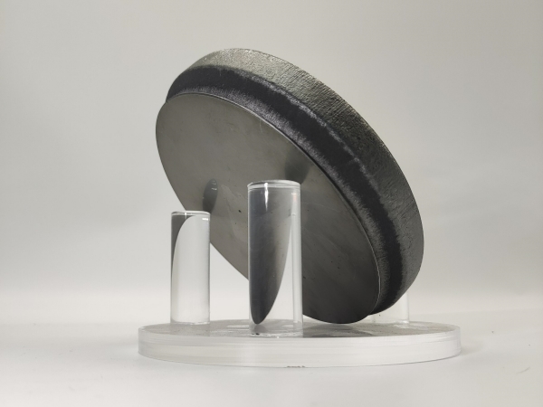
1. Technical Overview
Featuring superior comprehensive physical and chemical properties, diamond substrate wafers have emerged as core high-end substrate materials for third‑ and fourth‑generation semiconductor high-power devices, high-frequency RF devices, quantum optical systems, and precision sensing platforms. Compared with conventional silicon, sapphire, and silicon carbide substrates, diamond possesses ultra-high intrinsic thermal conductivity, excellent chemical inertness, ultra-broad spectral transmittance, and high dielectric breakdown strength. It effectively addresses critical industrial challenges of high heat-flux thermal dissipation, high-temperature oxidative failure, excessive optical loss, and elevated leakage current, making it the preferred substrate for next-generation high-performance semiconductors and optoelectronic devices.
Nevertheless, in heteroepitaxial growth systems, the significant surface energy and lattice mismatch between diamond and conventional semiconductor or insulating substrates results in extremely poor spontaneous nucleation capability. It is difficult to directly grow continuous, dense, low-defect, and ultra-flat diamond substrate wafers. Among various pretreatment strategies, electrostatic nano-diamond seeding technology exhibits distinct advantages including broad substrate compatibility, high process stability, excellent batch consistency, and scalable mass-production capability. It has become the most versatile and mature pretreatment process for polycrystalline
diamond substrates and ultra-thin diamond films in both scientific research and industrial manufacturing.
2. Core Technical Challenges of Diamond Growth on Heterogeneous Substrates
The primary bottleneck for diamond substrate fabrication lies in the difficult nucleation on heterogeneous interfaces. Diamond has a much higher surface energy than common substrates such as silicon, GaN, AlN, and sapphire. Under standard CVD growth conditions, carbon radicals struggle to stably adsorb, nucleate, and grow on substrate surfaces, leading to an extremely low spontaneous nucleation density ranging from 10 to 10⁵ cm⁻². Sparse and randomly distributed nucleation sites fail to support the growth and coalescence of continuous diamond films, readily inducing structural defects such as pinholes, micro-fractures, sparse grains, and grain-boundary voids. These defects further cause excessive surface roughness, deteriorated thermal uniformity, weak interfacial adhesion, and low device yield.
Accordingly, artificial pretreatment is essential to construct high-density, uniformly distributed, and structurally stable diamond nucleation sites on substrate surfaces. Electrostatic seeding serves as a critical process solution to overcome low nucleation efficiency on heterogeneous substrates and realize the controllable fabrication of high-quality diamond substrates.
3. Core Principle and Mainstream Implementation Methods of Electrostatic Seeding
Fully named nano-diamond colloid electrostatic self-assembly seeding technology, this process relies on interfacial electrostatic interaction to achieve uniform seed layer deposition. High-purity and well-dispersed detonation nano-diamond (DND) colloids are adopted as the seeding precursor. By precisely modulating colloid pH values, surface functional groups, and substrate surface electrification characteristics, the Zeta potential polarity and magnitude of both nano-diamond particles and substrates are regulated. Driven by electrostatic force, nano-diamond particles spontaneously adsorb and orderly arrange on various heterogeneous substrate surfaces, forming a uniform, dense, and monolayer pre-seeding structure. In the subsequent CVD growth process, the seeded grains grow vertically and coalesce horizontally, ultimately forming homogeneous, compact, and structurally stable diamond substrate wafers.
Three mainstream implementation methods are widely applied in the industry: immersion coating, spin coating, and electrospray seeding, each with targeted application scenarios. Spin coating is suitable for small-size, ultra-flat research specimens; electrospray is optimized for patterned and selective regional seeding; the immersion method stands out for its simple workflow, outstanding large-area uniformity, and superior stability. It is widely adopted for the batch fabrication of 2–6 inch large-scale diamond wafers in industrial mass production and routine scientific research.

【Figure 1】(A) Schematic of hexagonal close-packed model of spherical nano-diamond particles; (B) Theoretical seed density variation versus particle diameter
Under the ideal hexagonal close-packed arrangement, nano-diamond particle size directly determines the ultimate nucleation density. Ultra-fine 2 nm nano-diamond particles deliver a theoretical maximum seed density of 2.88×10¹³ cm⁻². Smaller particle sizes enable denser seed arrangement, finer grain structure, superior surface flatness, and lower defect density of grown diamond films. Restricted by actual colloid dispersion uniformity, particle size distribution, and substrate micro-roughness, the stable industrial nucleation density reaches 5–8×10¹¹ cm⁻², fully meeting the fabrication standards of high-precision
polycrystalline diamond substrates and ultra-thin diamond films.
In terms of process characterization, conventional AFM suffers from limited lateral resolution and cannot accurately quantify the initial single-particle seed density. Pure SEM observation of post-growth grain density tends to overestimate results due to secondary nucleation interference. Therefore, high-precision industrial fabrication requires combined characterization methods including ellipsometry and micro-morphology scanning to ensure excellent batch stability and parameter consistency of diamond substrate wafers.

【Figure 2】TEM image of 5 nm diamond powder showing particle agglomeration morphology
4. Critical Influence of Colloidal Zeta Potential Stability on Nucleation Quality
Colloidal dispersion stability is the decisive factor governing the final quality of diamond substrate wafers. Nano-diamond particles are insoluble in conventional aqueous and organic solvents and only exist as stable colloidal suspensions. The dispersion state of the colloid directly determines the uniformity of seed adsorption. Industrially recognized stable colloidal systems require a Zeta potential ranging from -30 mV to +30 mV, where sufficient electrostatic repulsion effectively suppresses particle agglomeration and sedimentation.
Conventional detonation nano-diamond inherently carries abundant oxygen-containing functional groups, presenting negative potential characteristics. After high-temperature hydrogenation modification, the particle surface is terminated with hydrogen groups and converts to positive potential. Through differential potential modulation, the electrostatic seeding process can precisely match the surface electrical properties of diverse substrates, including conductive, semiconductor, and insulating materials such as silicon, sapphire, GaN, AlN, and silicon carbide, achieving uniform and dead-zone-free seed adsorption.
Improper colloid management leads to severe particle agglomeration. Large agglomerated particles form micro-protrusions and defect sites at the substrate interface, which further induce excessive film roughness, local delamination and cracking, uneven thermal conduction, and stress concentration during subsequent growth. These defects significantly degrade the yield and long-term service stability of diamond substrate wafers.

【Figure 3】AFM morphology and height line-scan profile of silicon substrate after seeding treatment

【Figure 4】Zeta potential comparison between hydrogenated/oxidized diamond colloids and SiO₂ substrate at different pH values
5. Low-Density Seeding Optimization for Thick Diamond Films for High-Power Thermal Dissipation
For thick diamond substrate wafers applied in high-power semiconductor devices and high-frequency power module thermal management, conventional high-density seeding strategies face critical film peeling issues. Although high-density seeding is ideal for ultra-thin and ultra-flat film fabrication, excessive seed density induces severe cumulative thermal stress during the growth of hundred-micron-level thick diamond films. Unrelieved thermal mismatch stress easily causes large-area blistering, cracking, and delamination failure.
For high-thermal-conductivity substrates such as AlN and silicon, controllable low-density seeding at the magnitude of 10¹⁰ cm⁻² introduces uniform micro-void structures at the substrate-diamond interface. These microstructures effectively release heteroepitaxial thermal mismatch stress, significantly enhancing interfacial adhesion strength, mechanical stability, and high-temperature long-term service performance of thick diamond films. This optimized scheme perfectly adapts to long-duration high-load heat dissipation scenarios of high-power electronic devices.

【Figure 5】Schematic of diamond growth mechanism on AlN substrate under low seed density conditions
6. Core Process Parameters and Comprehensive Evaluation
Overall, electrostatic nano-diamond seeding technology possesses comprehensive advantages including wide substrate compatibility, excellent process universality, large-area mass producibility, controllable cost, and superior repeatability. It is applicable to insulating, semiconductor, and conductive substrates, and supports the mass production of 2–6 inch wafers and customized patterned substrates. It serves as the fundamental industrial process for manufacturing high-performance polycrystalline diamond substrates and functional diamond thin films.
| Core Parameters / Indicators |
Specification / Characteristics |
| Theoretical seed density (2 nm particles) |
2.88×10¹³ cm⁻² |
| Practical mass-production nucleation density |
5~8×10¹¹ cm⁻² |
| Stable colloidal Zeta potential range |
-30mV ~ +30mV |
| Applicable substrate materials |
Silicon, sapphire, GaN, AlN, and other conductive/semiconductive/insulating substrates |
| Applicable wafer size |
2–6 inch large-size wafers |
| Main applicable products |
High-precision polycrystalline diamond substrates, ultra-thin diamond films |
In terms of process adaptability, this technology covers the fabrication of polycrystalline diamond products for precision optics, semiconductor thermal management, microelectronic devices, and protective coatings. Its primary technical limitation originates from physical adsorption mechanisms, which cannot achieve controlled grain orientation, making it unsuitable for high-end single-crystal diamond epitaxy.
JXT provides professional supply of
single-crystal diamond substrates, polycrystalline diamond substrates, and customized diamond films with various specifications. We support personalized customization of different sizes and thicknesses, fully catering to university scientific research, enterprise device R&D, and large-scale industrial mass production scenarios.
Related products:
single-crystal diamond substrates:
https://jxtwafer.com/product/CVD-Diamond-Substrate/2025-07-24/1250.htmlpolycrystalline diamond substrates:
https://jxtwafer.com/product/CVD-Diamond-Substrate/2025-07-25/1251.htmldiamond substrates:
https://jxtwafer.com/product/CVD-Diamond-Substrate/